Views: 0 Author: Site Editor Publish Time: 2026-02-11 Origin: Site


While the world's attention is fixed on nanometers within silicon chips, an equally intense precision battle is raging outside the wafer. The march toward 2nm, 1.4nm, and beyond isn't just a lithography challenge; it's a macroscopic manufacturing crisis. The machines that create these chips—EUV lithography scanners, etching chambers, wafer handling robots—require components of such monumental scale, flatness, and cleanliness that they push CNC machining to its absolute physical limits. Here, machining isn't just making parts; it is enabling the fundamental tools of progress itself.
In semiconductor capital equipment, the performance of the final chip is directly gated by the precision of its tool's internal components. The requirements are non-negotiable:
Ultra-Large Scale Precision: Modern EUV scanner stages and metrology frames can exceed 2 meters in length, yet must maintain flatness and straightness under 1 micron (1 μm) over the entire span. This is the equivalent of laying a kilometer-long railroad track with a vertical deviation of less than a millimeter.
Thermal and Dynamic Stability: Components must not only be precise in a static, 20°C lab. They must maintain that precision while undergoing thermal cycles from cryogenic cooling to high-temperature baking, and while moving at high speeds with nanometer-level tracking accuracy. This demands materials and designs where thermal expansion is not just compensated for, but designed out.
Sub-Surface Integrity & Cleanliness: A microscopically fractured grain or embedded contaminant from machining can become a particle-generating site in the high-vacuum, plasma-rich environment of a process chamber. This leads to wafer defects, tool downtime costing over $1 million per day, and catastrophic yield loss. The machined surface and its underlying material structure are critical functional elements.

Machining for semi-cap equipment diverges radically from conventional aerospace or automotive work.
Material Extremes:
Invar / Super Invar: A nickel-iron alloy prized for its near-zero thermal expansion coefficient. It is notoriously gummy, difficult to cut, and highly work-hardening, requiring specialized tool geometries and rigid, high-pressure coolant systems to achieve optical-grade surfaces.
Silicon Carbide (SiC) Ceramics: Used for electrostatic chucks and wafer stages due to its stiffness, thermal conductivity, and vacuum compatibility. Machining SiC is an abrasive grinding process, demanding diamond tooling and exquisite control to prevent micro-cracking.
High-Purity Aluminum Alloys: For vacuum chambers and shrouds. They require mirror-finish internal surfaces (Ra < 0.05 μm) to minimize particle adhesion and outgassing, achieved through diamond turning and meticulous polishing protocols integrated with CNC milling.
The "Metrology-First" Machining Paradigm: You cannot machine a 1-meter part to sub-micron accuracy without measuring it in-process. This isn't probing; this is integrating laser interferometers, capacitive gauges, and autocollimators directly into the machining loop. The machine tool becomes a hybrid machining and metrology platform, constantly verifying itself and compensating in real-time for errors that would be invisible on a standard CMM.
Cleanliness by Design: The entire machining process is engineered for ultraclean output. This involves:
Dry Machining or Oil-Free Coolants: Where possible, to eliminate hydrocarbon contamination.
Sealed and Purged Machine Environments: To prevent ambient dust from settling on the workpiece.
Post-Machining Protocols: Automated ultrasonic cleaning and particle count verification become part of the final QC ticket.
EUV Lithography Components:
Reticle & Wafer Stages: The ultra-precise, magnetically levitated platforms that position masks and wafers. Their complex grid plates, full of coolant channels and magnetic circuit features, are masterpieces of 5-axis micromachining and deep-hole drilling.
Optics Barrel Modules: The colossal housings that hold and align the multilayer EUV mirrors. Their dimensional stability defines the optical path, requiring stress-free machining of Invar with interfaces accurate to a few arc-seconds.
Etch & CVD Process Chamber Components:
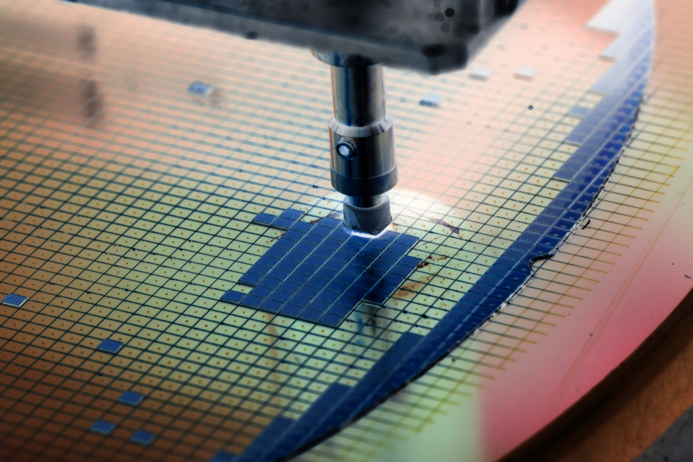
Showerheads: Perforated plates that distribute process gases uniformly. They may contain tens of thousands of micro-holes, each requiring precise diameter, taper, and surface finish to ensure uniform plasma and film deposition across a 450mm wafer.
Electrostatic Chuck (ESC) Bases: The SiC or aluminum nitride bodies that hold wafers with electrostatic force. Their cooling channels and electrode patterns are machined with tolerances that directly impact wafer temperature uniformity, a critical yield parameter.
Wafer Handling & Metrology:
Robot End Effectors: The "hands" that move multi-billion-dollar wafers. They must be lightweight, stiff, and non-particulating—often machined from specialized composites or ceramics with gentle, non-marking gripping features.
Metrology Frame Structures: The "skeleton" of overlay and inspection tools. Their long, thin beams must have near-perfect geometric stability, often achieved through iterative machining and stress-relief cycles that can span weeks for a single part.
In this domain, the CNC program and process parameters are not just instructions; they are core trade secrets. The know-how to consistently machine a 1.5-meter Invar beam to 0.8 μm flatness, without inducing stress, is as valuable as a patent. Leading machine shops serving this sector are not job shops; they are specialized process development houses. Their value lies in:
Material-Process Databases: Proprietary libraries of cutting data for exotic alloys and ceramics under cleanroom-like conditions.
Predictive Distortion Modeling: Finite Element Analysis (FEA) models that simulate machining stresses and predict final part geometry after stress relief, guiding the machining strategy.
Full Digital Traceability: Every cut, every measurement, every material batch is logged, creating an immutable record for part certification—a requirement for semiconductor OEMs.
The unspoken truth of the semiconductor revolution is that it is built on a foundation of macroscopic, almost unimaginable, precision. Each shrink in node size demands a corresponding leap in the capability of the tools that make them.
CNC machining for semiconductor capital equipment is no longer a metalworking craft; it is a discipline of applied physics, materials science, and extreme metrology. The shops that succeed here operate at the confluence of these fields, solving problems that define the boundaries of what is physically manufacturable.
Is your supply chain equipped for the precision demands of the Angstrom Era? Our division is dedicated to machining the foundational components of advanced semiconductor manufacturing.

 English
 简体中文
简体中文